How to Design a PCB for Manufacturing DIY Projects
July 28, 2021Today on the hookup I’m going to show you can take your hacked together DIY projects (or other people’s projects) and make them look professional by building custom PCBs. I’m going to walk you through all the steps and everything you need to know to make your first PCB. You don’t need to be an electrical engineer, and the process is easier than you think.

It doesn’t matter how simple a project is, if it looks like this some people are always going say it’s too complicated, or that it’s a fire hazard, or both. In almost all of my DIY project videos I get people commenting that I should just make them and sell them myself, but there are three big problems with that 1) I don’t want to have to deal with returns and warranty claims 2) If I was fairly compensating myself for my time investment it wouldn’t be the sweet deal that the DIY project is, and 3) Most of my projects don’t exactly look “professional”, and even though they are perfectly safe and reliable, they definitely look DIY… But PCBs are the answer to that.
Printed circuit boards or PCBs are not complicated. They’re just a non-conductive material with either holes or pads for mounting your electrical components, and then small embedded connections called traces that connect the components together. So, basically THIS is the exact same as THIS, but a lot nicer looking. Just to get everyone on the same page, lets talk about the 3 basic parts of a printed circuit board:
There are two ways to attach a component to a circuit board: There’s surface mount, where you have little copper pads on the board and you lay the components on top, and then there’s through hole where you stick the ends of the components through the board and then solder them from the bottom. If you’re new to PCBs and new to soldering, then through hole is the way to go, but the components tend to be bigger, so your design won’t be as compact.
Speaking of soldering, on your PCB you don’t want solder everywhere, you only want it around your components. So to do that, the rest of the board, including the traces, is covered in a thin lacquer called a solder mask that prevents solder from sticking to it, leaving the solder only where you want it.
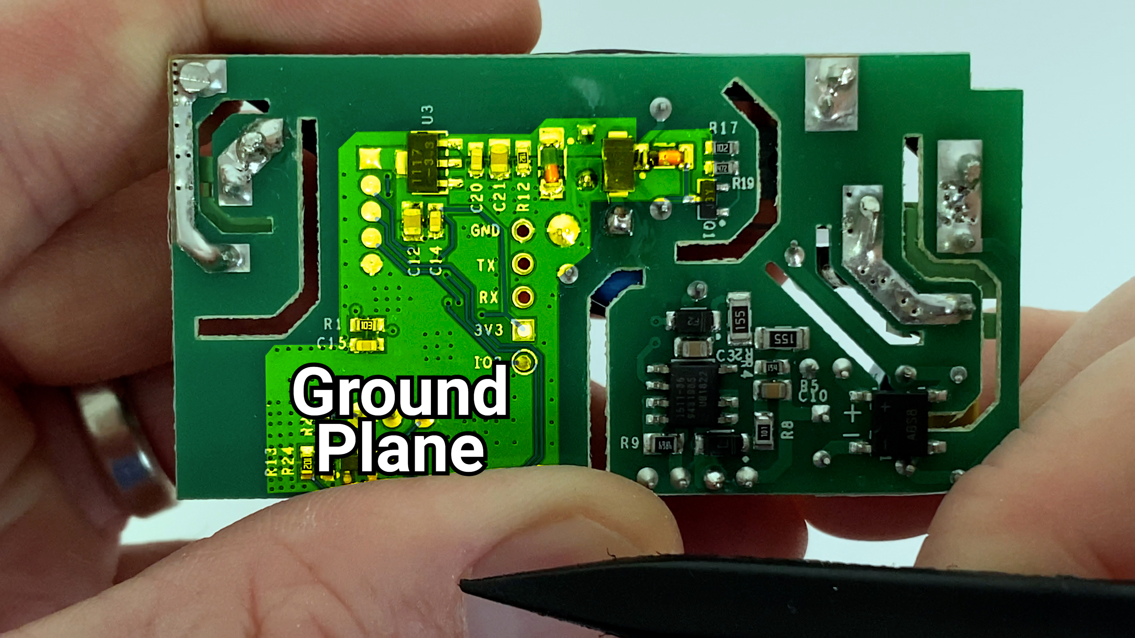
As for the traces, most pcbs are double layer, meaning the tiny copper lines that act like wires between the components can be on the top, or the bottom. When you have a lot of traces to route around the board a double layer PCB makes it easier to do since traces can’t cross over each other. The traces can also go from the top to the bottom of a PCB and any time you see a small hole without a component in it, those are called via’s and that’s how the trace gets from one side to the other. Traces also work just like wires, where if you are sending a lot of amperage through one trace it will need to be thicker than a trace that is just carrying data, so some traces are wider than others and therefore use more copper. Additionally it’s common for a PCB to have an entire ground plane which means that anything that isn’t a trace is actually connected to ground. Ground planes are good because they reduce electrical noise and help with head dissipation, but they aren’t completely necessary. I’ll show you how to make one in this video, but it’s probably overkill for our board design.
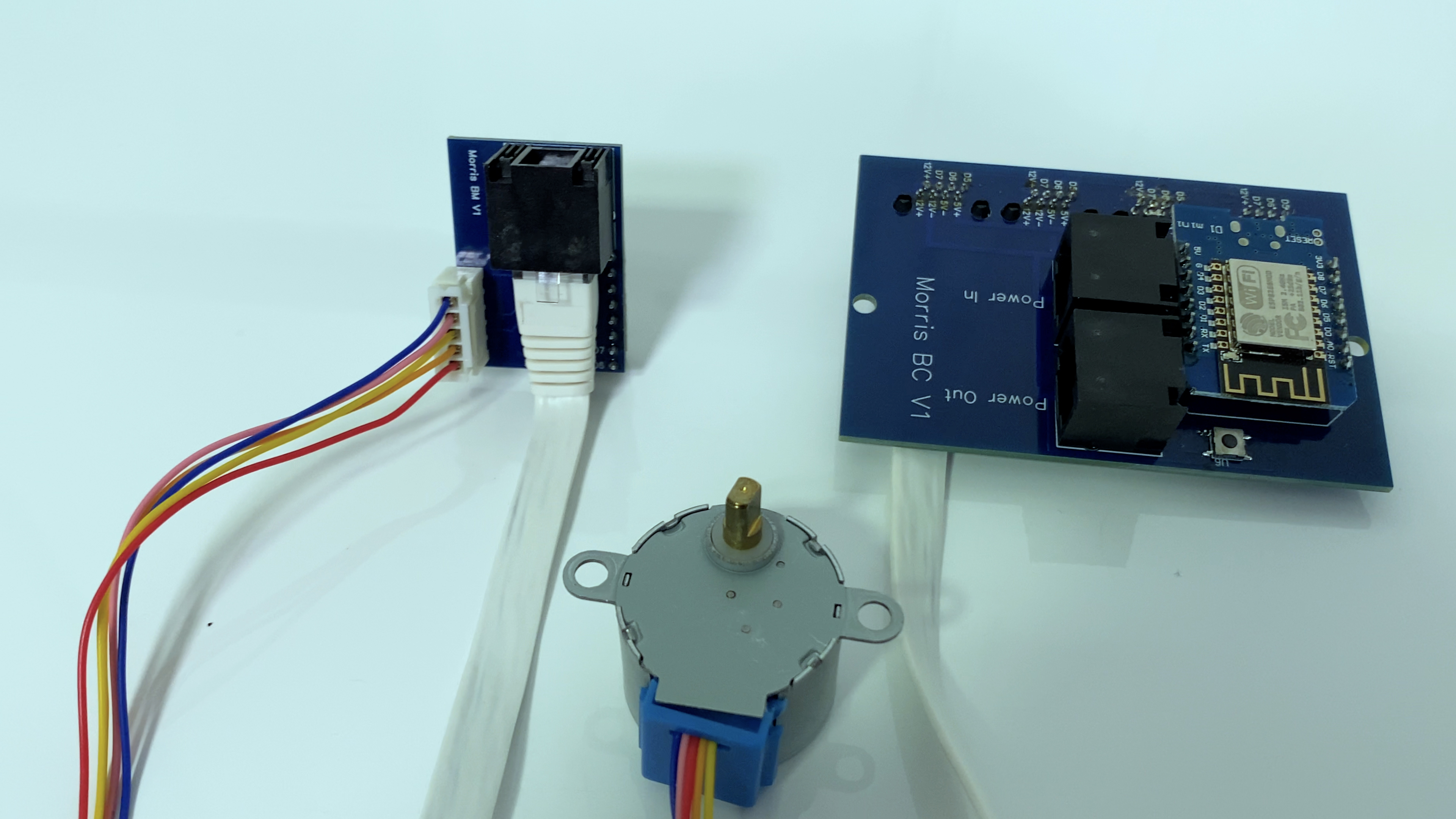
So now that we’ve got the basics down, lets take a look at a few PCBs to see what I’m going to show you how to make today. This board is an LED controller called the dig-quad made by a youtuber named Quindor. You can see that the bottom side of the board is composed of through hole components, as well as surface mount components. Not only that, but quindor has designed all kinds of circuits to do voltage regulation, logic shifting, power smoothing and other crazy stuff. Even though that may be your ultimate goal, that’s not what we are doing today. Today, all we’re going to do is take pre-made components and connect them together using a PCB instead of wires, turning something like this, into this.
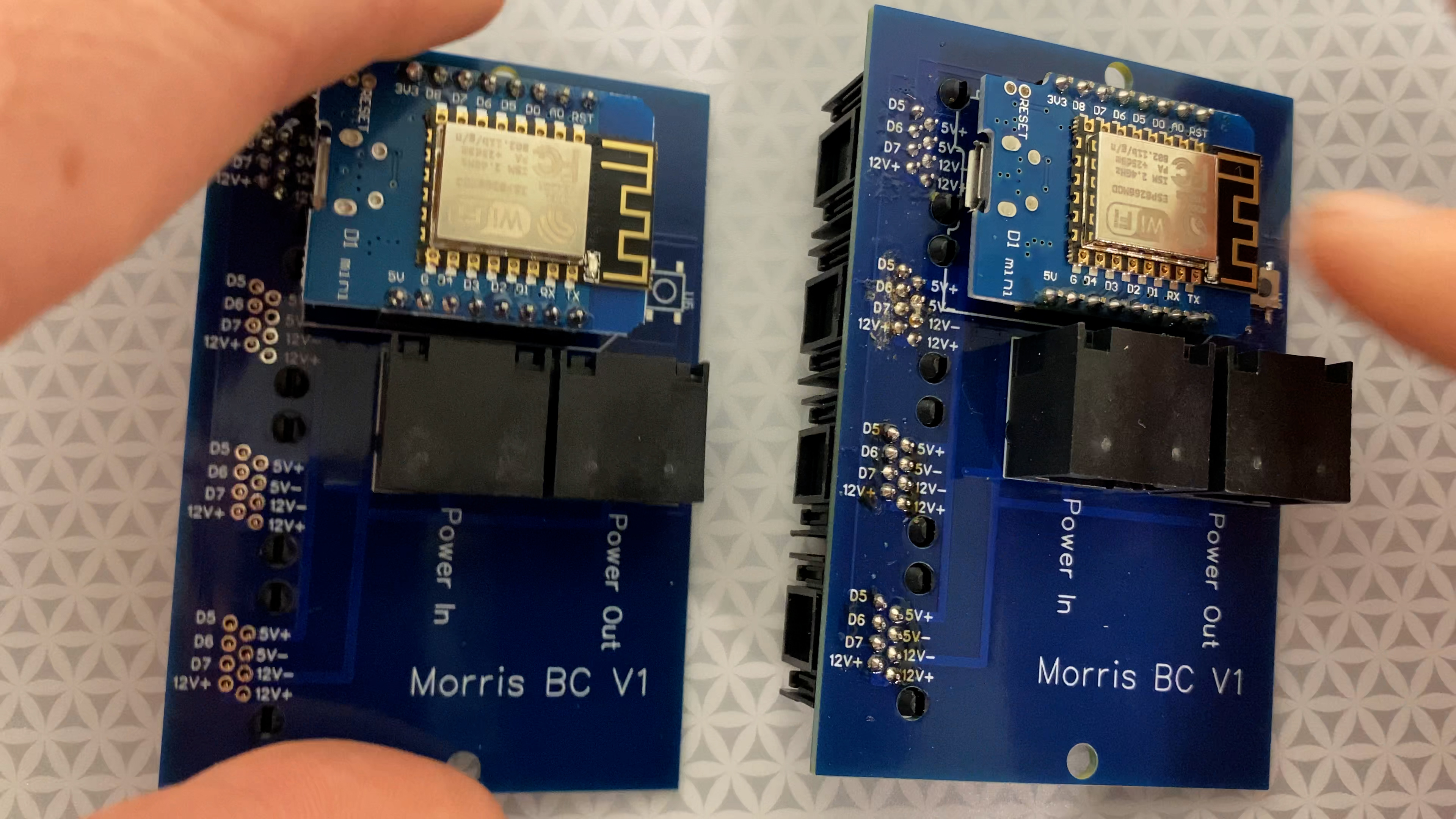
The software that we’re going to use is EasyEDA which is a free online PCB designing service with thousands of parts in its database to make the process of PCB creation easy. Step one is to log into EasyEDA, and I’m going to use my google account to do it. After that go ahead and make a new project. I’m going to be making a PCB for my blinds project, and specifically I’m going to take inspiration from a few PCBs that my subscribers have made and I’m going to make a sender board with 3 ethernet jacks, and a receiver board that goes in each of the blinds.
After you choose a name for your project, EasyEDA will automatically open up in schematic mode, and schematic mode looks a little confusing, but don’t freak out. As I said before, easyEDA has a bunch of pre-made parts, so I’m just going to start searching. For the sender board I’ll need a ESP8266 NodeMCU, a buck converter, a screw terminal, and a few ethernet jacks. I’ve had pretty good luck just searching for the part number listed on the amazon page, and sometimes when searching you’ll find an official part from EasyEDA or LCSC, but most of the time you’ll be using user contributed parts, which I’ve found to be pretty reliable.
Since we’re using common components I ju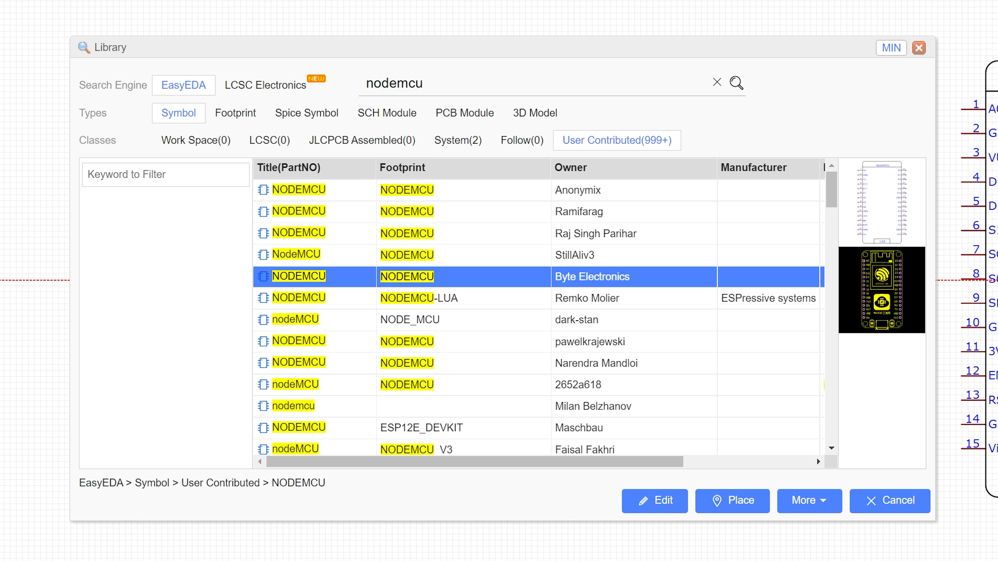 st ordered them from Amazon, but could also order from a proper electrical components company like LCSC if you are making a large order, or you just can’t find the right part for the right price on amazon.
Once you’ve got all your parts on your schematic you need to make your connections. It’s not super important to make your connections look nice here, but it does make it easier to keep track of them. Don’t worry about overlapping connections on this page, this isn’t how the traces of your PCB will actually look.
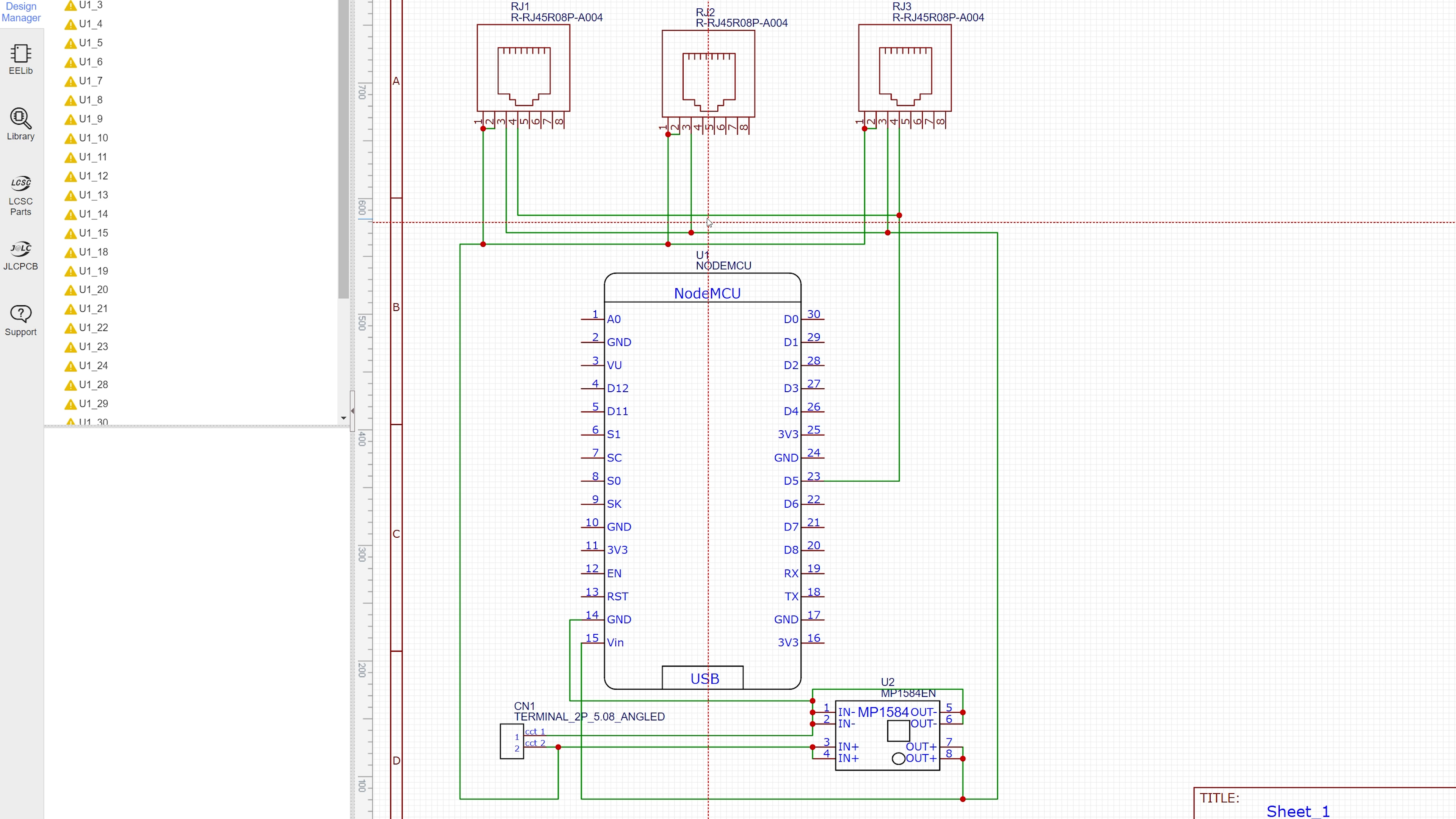
Once you’ve got your connections done use the labels for VCC, ground, and 5V and any other connections that you want to label and then save your project. Next click on the Design menu, then convert to PCB. It will probably tell you that some of your nets are not connected, and that’s to be expected. Nets are the term used for the connections between the pins on your PCB. In our case we only used a small fraction of the pins available on the NodeMCU so the rest of the nets for those are open. If you labeled all of your connections you should be able to see that the unfinished nets aren’t part of the connections that you need so go ahead and click “No, keep going” to get to your PCB Page.
On this page you can keep the default settings and then position your components how you want them on your final PCB. For me, I want the ethernet jacks on the back of the board and the nodemcu, buck converter and terminal block on the front. To do this, select each component and change the layer dropdown to your desired location. There are a bunch of layers to choose from, but the important ones for placing your parts are Top Layer and Bottom Layer, which are copper layers located on the top and bottom respectively.
At this point I also like to label my board. You can not only put new text on your board, but you can edit the text that imported with your parts, and you can change or remove the component labels that were automatically generated. These labels should be part of either the top silk screen or the bottom silk screen, since we want them labeled with ink and not copper. I’m going to put some general instructions on my board, label the positive and negative terminals of my 12v connector, and assign an ethernet port to each window.
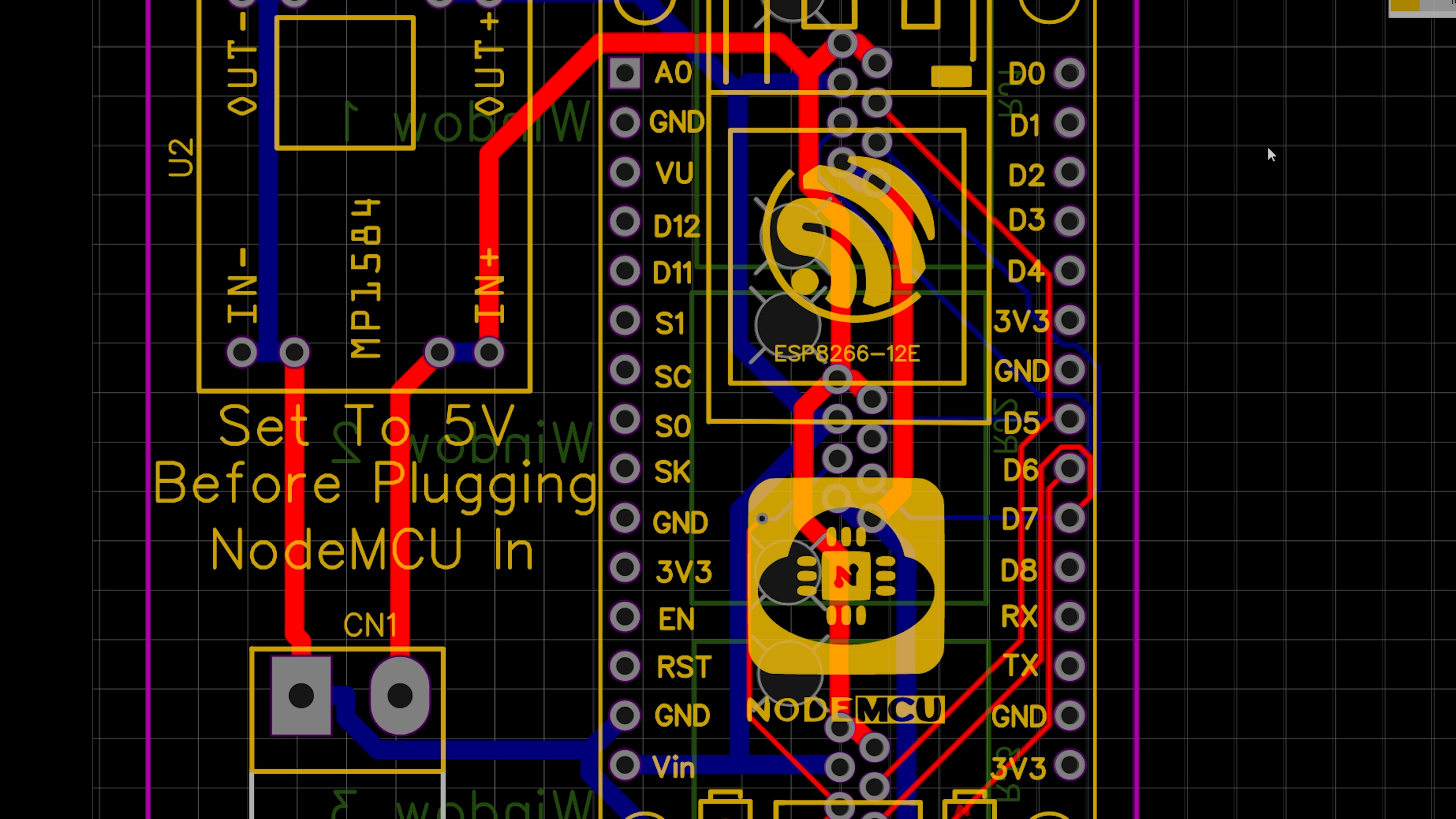
Last, it’s time for routing… which is figuring out a way to get all your traces connected without overlapping each other. For complex boards with a bunch of small parts routing is an art form, and for some things like antennas the length, shape, and location of the traces has a huge effect on performance, but for our board we can just use the auto router. Go up to the route menu and select auto route. If your board isn’t going to carry a lot of power you can just leave the default settings and hit run, but since we are carrying a decent amount of current on our 12V VCC line I want to make those traces extra thick. To do that I’ll create a design rule for that specific net by hitting the design rule button, creating a new routing rule with thicker traces, and then assigning that rule to my 5 volt and VCC and ground nets. After the rules are set hit run and the auto router should do its thing. Sometimes it goes a little crazy and creates squiggly lines, if that happens you can remove any unnecessary turns by double clicking on the white anchor point on that turn.
If you wanted to create a ground plane instead of thick traces you’d select the copper area tool, tell it you want to apply that copper plane to your ground net and then draw whatever area you want. Again, for this project I’m just going to use traces for my grounds.

After routing give your board one last look over. I like to look at each layer individually by clicking on the eyeball on the layers menu and I zoom in make sure all the parts are aligned and all the traces are connected where I want them, then hit save. Next, to actually get them printed you will need to generate a gerber file, which is actually a collection of files used to tell your PCB manufacturer how to make your boards, so click on fabrication, then pcb fabrication file. It’s going to recommend that you check your file to design rule violations, which is probably a good idea. In the next menu click generate gerber to download a zip file containing all the instructions for your PCB.
This zip file can be used with any PCB manufacturer, so I’m going to use PCBWay since I’ve always had great service from them, they support my channel, and their prices are competitive.
At the PCBWay website enter the length and width of your pcb into the instant quote window, then on the next page you can select your shipping method and change any other settings that you want, like the color of your board, and then add to cart. On the next page you’ll upload your gerber file and then one of PCBWay’s employees will review your order to make sure there are no serious design errors before sending it for production. Check out the description of this video, I usually have a promo code to get at least a few dollars off your first order at PCBWay.com
PCBWay makes your PCBs quickly, but how fast it gets into your hands depends mostly on the shipping method you use. When your PCB order arrives it’s time to get soldering, and since this is all through hole stuff it’s a great way to practice if you are a novice. The key to soldering through hole components is to try not to touch the solder with the iron, instead press the iron against the pin and the hole on the PCB and then touch the solder to that. If you screw up and get a bead of solder you can always go back and hit it again with the iron and your solder blob should turn into a nice tent, like this. Another thing you can decide at this stage is whether you want your parts to be permanently attached, or if you want to use female header pins to be able to remove and switch out parts as needed. Header pins are an extra cost, but they are well worth it in my opinion if you can spare the extra height.
So here it is the “Hello World” of PCB Making, and a gateway drug into more complex circuits and professional looking projects. This PCB was actually made by a subscriber and posted on the hook up facebook page. If you’ve made one of my projects into a PCB I’d love if you could come share it with the group. I’ve got links down in the description to a few projects made by my subscribers and the gerber files for the PCBs from this video. I’m definitely not an expert at this yet, so if I missed something important make sure to leave a comment and let me know. Thank you so much to all my awesome patrons over at patreon for your continued support of my channel. If you’re interested in supporting my channel please check out the links down in the description. If you enjoyed this video please consider subscribing and as always, thanks for watching the hookup.